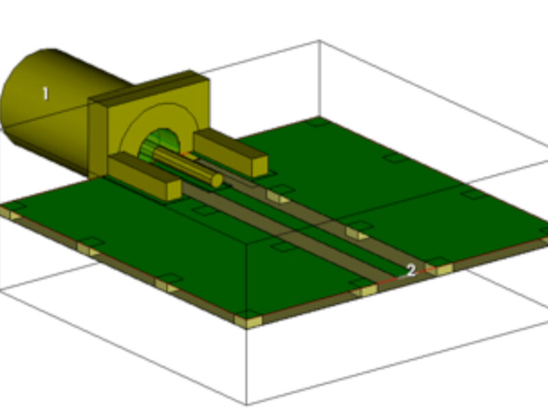
Coaxial connector to microstrip transition optimization
When comparing measurement results to simulated ones, the transition (Figure 1) from the measurement hardware’s coaxial cable to the signal trace of the DUT is commonly assumed to be ideal. But in reality, this “ideal” condition results in data mismatch (simulation data =/ measurements) at higher frequencies.

This ideal assumption is implicitly made as soon as the simulation input/output ports are on the trace, e.g., on the microstrip or coplanar waveguide (Figure 2). While there are multiple methods that can be used for ensuring the transition has as little reflection as possible, this specific example highlights the approach of using a full 3D FEM EM model for the connector. Doing so enables the treatment of the transition’s parasitics in an analytic fashion and moves us away from the “ideal” and toward reality.

Figure 2: Typically the simulation port is directly on the microstrip, neglecting the discontinuity represented by the connector in Figure 1, and thus systematically distorting the simulated versus measured results.
The design
In the schematic (parent document), we have drawn a printed circuit board (PCB) with the signal trace. The 3D connector that is designed for 20mil substrates is, technically speaking, a sub model (or child) of the parent document, i.e., the design is hierarchical. The connector model allows for the placement of a port on the coaxial cable end of the connector (input port), and for the other port to be defined as a regular wave port at the end of the microstrip (output port). The reference plane of the output port is moved just after the connector.
Transition quality without optimization
Looking at S11 (Figure 3) of the transition reveals that the inherent matching is good only up to about 2 GHz. At the target design frequency of 10 GHz, the reflection is as high as -10 dB. Clearly the design would now benefit from an optimized transition – not only because of lost energy, but also because the mismatch is a considerable source of error for the measurement versus simulation.

Figure 3: Reflection coefficient of the transition at coax port before optimization. Click image to enlarge.
Optimization strategy
The transition model can be optimized in a schematic using the EM document as a regular sub model. It is easy to determine that a series-L parallel-C matching circuit would do the optimization job at 10 GHz. In microstrip, a series-L can be realized by a narrow segment of strip, while a parallel-C can be realized by a wide strip segment. It is straightforward to optimize the required strip dimensions, as shown in Figure 4.

Figure 4: Matching circuit candidate to optimize transition from coax to microstrip. Click image to enlarge.
The final step is to put the matching circuit dimensions in the 3D model and run a verification simulation, as shown in Figure 6.

Figure 5: Reflection coefficient of the transition at coax port using the closed-form models of the matching circuit (green curve). Click image to enlarge.

Figure 6: Reflection coefficient of the transition at coax port including a full 3D model of the matching circuit geometry (blue curve). Click image to enlarge.
It can be seen that the first matching attempt is excellent.
It is also instructive to view and animate the surface currents at 10 GHz, as shown in Figure 7.

Figure 7: Surface current annotation of the optimized transition at 10 GHz.
To summarize, such a simple matching circuit provides signal transmission from coax cable into microstrip with less than -20 dB reflection at 10 GHz target design frequency. The matching bandwidth is about 2 GHz, and it is easily and reliably optimized using conventional circuit models with the connector EM model. A full 3D EM verified solution is readily available with the optimized geometry.
Various transition models from different connectors to different board substrates can be stored as a library, and conveniently used in any subsequent circuit design. Integrated 3D EM tool enables keeping all design data within one AWR Design Environment™ (AWRDE) project file, including connectors, bonded packages, housing or any other arbitrary 3-dimensional objects. This eliminates the risk of model misuse e.g. in case where a horizontal connector is changed to a vertical; the graphical view of the design layout immediately reveals which 3D model is used, unlike in the case where the S-parameters of the connector are evaluated elsewhere and imported as a blind file into AWRDE. Single project file also means easier documentation, design transfer, storage and reuse.
Watch this video that goes into detail regarding this topic: full 17 minute clip or software only 4-minute demo within this clip.
 If you enjoyed this article, you will like the following ones: don't miss them by subscribing to :