Design: Multimode, multiband transceiver technology delivers LTE
With the introduction of smart phones and tablets, mobile data transmission has grown dramatically over the last five years. The Long Term Evolution (LTE) standard improves spectrum utilization efficiency, increases speed, and handles greater data traffic. Success of LTE technology is tied to an ecosystem development that must take place at the same pace—or faster—than that of the infrastructure implementation.
Due to an expected explosive growth of data usage, it has become imperative for operators to make effective use of spectrum and implement LTE as quickly as possible with an ever-increasing number of bands. This is a challenge for transceivers. The 3rd Generation Partnership Project (3GPP) has responded by coming up with a unified approach to FDD and TDD technologies. Currently, the wireless communication spectrum (up to 3.8 GHz) is separated into 43 bands; bands 1 to 32 are classified as LTE-FDD and bands 33 to 43 are classified as LTE-TDD.
From a transceiver standpoint the challenges are:
- Multiband: such a plethora of LTE bands necessitates a multiband transceiver.
- Multimode: roaming requirements in legacy operating networks (WCDMA, EVDO, TD-SCDMA, CDMA and GSM) require transceivers to be multimode.
- Dual technology: transceivers need to support both TDD and FDD technologies.
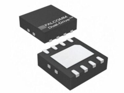
Transceivers for 0.7 to 2.7 GHz spectrum need to handle both FDD and TDD technologies in order to cover FDD bands 1-32 and TDD bands 33-41. Currently available state-of-the-art transceivers support all of the above bands with multiple ports available from a single RFIC (see Figure 1). This requires significant processing power. In the case of the Fujitsu RFIC shown in the figure, the processing requirement is addressed by distributing the load between the baseband and transceiver. For example, the transceivers are embedded with ARM® processors that reduce baseband processing requirements. This, in turn, reduces power consumption and improves response time for dynamic adjustments.


In addition to being multimode and multiband, today’s multi-featured RF transceivers need features such as:
- Low power consumption
- Small size (for both the transceiver and the RF front end)
- Standards-based baseband interface
- Flexible RF interfaces
- Carrier aggregation capability
- Compliance with 3 GPP standards
Low Power Consumption
Modem power consumption depends on the mode of operation (2G, 3G, 4G), technology (TDD, FDD), band use and 3GPP requirements. The transceivers, the baseband chipset and the RF front-end components must consume low power in all modes, individually and collectively. Flexibility and ease of programming for all the modem components are critical to achieve these goals.
The primary factors that govern power consumption for the transmit path are:
- Power output
- Power amplifier (PA) efficiency in max-power and backoff modes
- Linearity, adjacent channel power leakage ratio (ACLR) and noise performance.
Factors that govern power consumption on the receive path are:
- Dynamic range of the receiver
- Power consumed by the low-noise amplifiers (LNAs)
Within the RF subsystems, PAs are the major source of power consumption. Efficiency of the PA is greatest in the high-power saturated mode of operation. Most vendors cite their efficiency data based on this mode. However, efficiency drops when power is backed off, as the DC bias to the PA is only optimal at high power, leading to inefficient operation of the PA at a normal backoff power.
Partly to address the inefficiency at backed-off power, we are working on transceivers that could take advantage of a technique called envelope tracking (ET). ET allows the DC bias to be optimized in real time for the desired power reduction, while maintaining good PA efficiency numbers. The ET feature is illustrated in Figure 2.


Typically, ET optimization realizes a 20 to 30 percent reduction in power consumption.
To comply with 3GPP requirements for different bands, the transceiver has to be optimized for linearity, ACLR and CIM3 in each band. For this optimization, the transceivers must be easily programmable with ample processing capability. This flexibility with high-level API also allows multiple bands to be driven through a single port.
On the receive path, an enhanced transceiver design that eliminates the need for LNAs on the front end is ideal. With multiple-band support, elimination of LNAs and SAW filters reduces power consumption as well as component count and footprint.
Power consumption can vary based on the dynamic range requirements. Receivers with high dynamic ranges require high linearity, which increases power consumption. Conversely, receivers with low dynamic ranges need less linearity and therefore consume less power. Transceiver programmability provides the flexibility needed to optimize for each situation.
Programmable transceivers that enable flexible RFIC configurations allow manufacturers to customize various settings and optimize tradeoffs for customers. These transceivers can manage power requirements for various elements including operating mode (GSM, WCDMA and LTE), phase noise, linearity, and ease of calibration. Unlike non-programmable transceivers, such optimization does not require any hardware changes, which allows for scalability and re-use with only firmware changes.
Another common element that governs power consumption is the voltage-controlled oscillator (VCO). Power consumption of the VCO increases with reduced phase noise. Thus, phase noise adjustments can be made to hit noise targets that achieve 3GPP compliance. Tuned transmission lines can reduce the number of LO buffers required and further reduce power consumption.
Compact Transceiver and the RF Front End
A streamlined design results in lower component counts and reduced size, both of which are essential for modern smartphones and other user devices. Original device manufacturers (ODMs) value such designs as they make it possible to make smaller units and/or provide more band support.
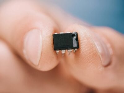
The elimination of LNA and matching networks in the RF front end reduces the component count and the RF front-end footprint. For example, in a Fujitsu prototype board supporting pentaband LTE, pentaband 3G and quadband 2G configurations, the entire RF portion (including the transceiver) occupies approximately 350 square mm (see Figure 3).


Standards-Based Baseband Interface
The interface between the baseband and RF is generally an analog I/Q or an open-standard MIPI serial digital interface. When vendors develop a system on chip (SOC), they often use a proprietary interface. However, an open standard interface offers more advantages.
For example, with transceivers supporting the MIPI DigRF standard, the RF chip can be interfaced with baseband chips (MIPI DigRF standard) from multiple vendors, giving the ODM flexibility to choose the digital baseband (DBB) provider. The MIPI DigRF serial interface also reduces the number of pins required for the interconnection between the baseband and RFIC. Fewer pins for the RFIC make it easier to design the RFIC in smaller packages and to reduce the layout size of the RF subsystem. The advantages of this feature are illustrated in Figure 4.


Flexible RF Interfaces
Optimal matching of all components in the RF front end determines the efficiency of the RF path. For example, the RF PAs should be chosen based on their ACLR and efficiency. In addition, transceivers must be capable of controlling the amplifier power performance effectively. One way to achieve such control is to incorporate detectors matched for different modes (such as peak, RMS and linear detectors 2G, 3G and 4G). Inclusion of such detectors in the programmable RFIC allows for flexibility and reduced component count. RF front-end control can be achieved with MIPI or GPO interfaces.
Based on band coverage needs, a careful carrier-interference analysis is necessary to arrive at the required receiver sensitivity and duplexer rejection characteristics. The choice of the RF front-end component should be made holistically, based on the transceiver-sensitivity limitation and duplexer-design characteristics. Over-specifying requirements for one RF component, without considering the capability of the other RF components, only drives costs higher and lengthens the development cycle.
The antenna is also a part of the critical RF path. Antennas have to cover 700 MHz to 2.7 GHz. They have to be broadband, which compromises VSWR performance and gain. Automated front-end tuning features in the transceivers can improve performance by better matching each band of operation.
Carrier Aggregation
3GPP release 10 will have carrier aggregation (CA) requirements in both the intra-band and inter-band spectrum. RF transceivers should be able to support the CA requirement, which could include broader LTE bandwidth up to 40 MHz. Our current approach, illustrated in Figure 5, provides CA with two transceivers, which presently support 20 MHz bandwidth.


Future transceivers are expected to provide an even larger bandwidth capability up to 60 MHz in a single RFIC. Transceiver vendors indicate that such single RFIC capability will become available within 12 to 24 months. The main engineering challenge is to develop front-end components that help reduce second and third harmonics, and other intermodulation products, which meet 3GPP requirements.
In conclusion, future transceivers must be designed with dual technology (FDD and TDD) multiband and multimode capability as well as excellent receiver sensitivity. The transceivers must also have the flexibility to work with baseband chipsets and RF front-end components from different vendors. Such programmable transceivers provide the scalability and re-usability required to service a large segment of the market.
About the Authors:
Ganesh Krishnan has a bachelor’s degree in electronics and communication and a master’s in business administration from Keller Graduate School of Management. He has more than 17 years’ experience in the wireless field, and has held product manager positions with Radio Frequency Systems (Alcatel), Powerwave Technologies, Huawei and now with Fujitsu Semiconductor Wireless Products.
Claudio Rey received his bachelor’s and master’s degrees from UBC and his doctorate from McGill University, all in electrical engineering. He has worked in the wireless industry on digital predistortion of base-station power amplifiers, on wireline and wireless modems and, most recently, on transceiver system and architectures for WIFI/cellular 2G, 3G and LTE.
 If you enjoyed this article, you will like the following ones: don't miss them by subscribing to :